AIS339 Chameleon

Description
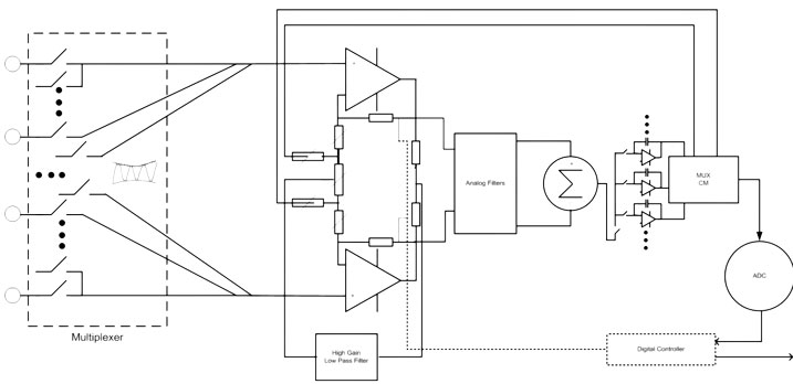
The AIS339 Chameleon is an AFE designed to enable signal capture in difficult real world environments. Baseline capture, common mode accelerated recapture, noise rejection, nuisance signal nulling, multi-order analog filtering, and an up to3rd order almost all pass (Bessel) with mHz bandpass low end corner are example capabilities. To accomplish this the AIS339 includes: i) five input channels and a single reference channel; ii) a programmable gain amplifier (PGA);iii) differential voltage input or transconductor current mode input; iv) a high common mode rejection driver; v) a fast programmable local loop to allow fast capture & recapture of the common mode; vi) a sample and hold circuit allowing fast recovery from events which move the baseline; viii) an up to 6th order ]high order programmable filter response; ix) a buffered differential voltage input between the negative terminals of the instrumentation amplifier to null nuisance signals*; x) analog or ADC outputs; xi) an optional two terminal common mode driver; xii) amplifier offset and shift registers. Between the amplifier and the ADC the AIS339 compares to sigma delta solutions with an ENOB of 18 bits but requires substantially less current. The AIS339 is capable of nyquist rate sampling between multiple different sensors*.Sample & Hold and fast drift recovery circuitry is provided to remember each sensor’s common mode and return to it when a channel is selected. Also included is a precision on chip analog reference and charge pump to maximize the input common mode range. The AIS339 will operate with a supply voltage as low as 2.7V up to 3.6V and is available in a5x5x0.75 48-pin QFN package. *Patents issued or Pending
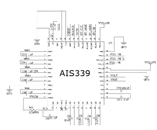
AIS339 Typical Circuit
System Features
- Offers multiple systems to ease capture of sensor data:
– Programmable Gain Amplifier (PGA)
– up to 18 bit ENOB overall accuracy (between Amplifier & ADC)
– 120dB CMRR rejection
– SPI based time constant loop adjust for fast signal recapture
– INA tap to allow nulling, lattice wave prediction or DSP in the loop
– Baseline Sample & Hold for each channel to allow multi-channel nyquist rate sampling
- Allows Closed Loop DSP Around INA
- 6 Input (5xMultiplexer, One Ref Channel)
- Voltage Gain or Transconductor Mode
- Low Noise INA with Digitally Programmed AGC
- SPI Interface
- Charge Pump to expand Input Range
- Precision Analog Reference
- 10-Bit ADC with Separate Enable/Fast Wakeup
- Multi-order Bandpass Filter Response
- 150uV Maximum Offset Voltage
- 5uV inband input referred noise
- 170uA Supply Current
- 48 pin QFN 5x5x0.75
Applications
- Optical PPG (Pulse) or Electrical (ECG) sensing
- ECG, PPG, SPO2, Biometric Extraction
- Heart & Muscle ID
- Real time wavelet processing
- Gas Sensors
- Vibration Monitoring
- Audio Monitoring
Product Description
The primary subsystems are as follows:
- Five Input Differential Multiplexer
– Full Channel Sample & Hold
- Input Instrumentation Amplifier
– Programmable Gain (PGA)
– 5uV Input Referred Noise
– 150uV Trimmed Input Offset
– Programmable Common Mode Feedback Loop(102dB CMR)
– Common Mode Loop Time Constant Acceleration
– Charge Pump to Maximize Input Range
- On Board Terminator (120dB CMR)
– Integrated Resistors
– RLD return without a Third Terminal(Programmable)
- Filters
– Integrator Loop Around Amplifier Chain (LFPole)
– 3rd Order MFB Filter (Component Configured)
– Programmable Differential to Single Ended Conversion
- 10 bit ADC (up to 12 bit with multiple sampling)
- Overall ENOB=18 bits compared to Digital Solutions
- Analog or Digital Single Ended Output
Multiplexer
The AIS339 accepts up to give input channels (CFx) against a single reference channel (CFB). Connecting a differential input signal to these inputs allows multiple signal paths to be connected to the gain, filter and digitization path of theAIS339 relative to the same common terminal. This can be useful for example in applications like a five lead ECG.
To choose the input channel CFx, write the channel number to be coupled to the first three bits of the Config 1 Register(0x4) as illustrated in Figure 1.
In addition to selecting the multiplexer, the AIS339 contains a number of sample of holds across the entire signal chain corresponding to the desired channel. The purpose of these sample and holds is to hold different nodes throughout the signal chain to their previous values the next time that the channel is selected. This reduces any exclusions if one returns to the channel which could otherwise cause glitches or delays in recovery. It also allows nyquist rate sampling such that the AIS339 may be used for multiple channel continuous signal acquisition even though it only offers a single signal path, saving money vs. others solutions. For example, in a five lead ECG the AIS 339 can be used to continuously acquire ECG data from five leads ”simultaneously” not just one channel at a time, replicating a system which otherwise would require five distinct channels and the costs involved therein. As most biometric signals are slow, the multiplexer and sample and hold circuitry can be switched at or above the nyquist rate required to reconstruct the signal from the digital sample.
Figure 2 further illustrates the Sample and Hold system. The multiplexer itself provides a sample and hold capability at the input and other nodes such as the integrator differential loop are separately held. When a previously used channel is selected the previous values are reapplied so that the loop can return to its previous value prior to actuating the multiplexer to the input channel. In this way we do not lose the common mode of each channel and do not have to recapture the operating point.
Offset & Noise
The AIS339 is trimmed to ensure a very low input offset voltage, and designed to minimize input referred noise. Specifically, the AIS339 is trimmed to approximately 150uVof input offset voltage, making it ideal for measuring extremely small signals such as ECG or EEG. Input referred noise will vary with the gain settings of the system, however, typical values are as shown in Table 1.
Table 1. Input Referred Offset at Various Settings
Differential Signal Channel Gain
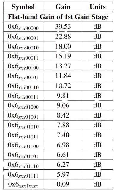
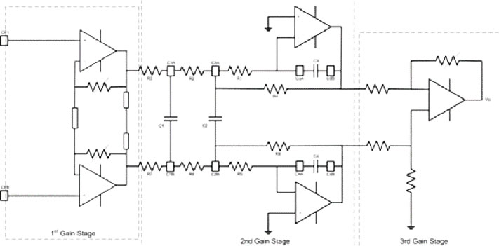
Figure 3 shows the three gain stages representing the differential path of the AIS339. The AIS339 accepts one of five multiplexer inputs into the CFx pins, with the other differential input being the CFB pin. The first gain stage is an instrumentation amplifier (PGA) with programmable gain. The second gain stage is fixed by the an MFB filter. The final differential to single ended buffer stage with programmable gain. The output of this stage is buffered to an analog output and also presented to the internal analog to digital converter. At maximum gain, the overall equivalent ENOB compared to a fully differential converter is 18 bits. In other words it would take 18 bits of accuracy from a completely digital ADC to match the combined gain and ADC of the AIS339. The first stage flat-band gain settings are shown in Table 2

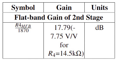
The second gain stage, the MFB filter, has a fixed gain which is shown in Table 3. To program the gain set R4MFB to the desired gain according to R4MFB/1870 but ensure that filter coefficients are re-calculated.
The third stage of gain, the differential to single ended converter, has can be set per Table 4.
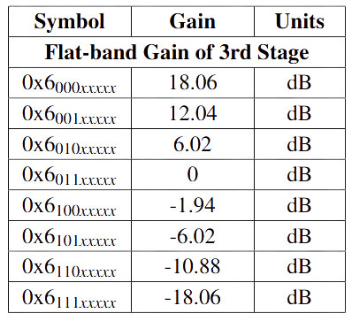
The overall DC gain can be calculated by adding the 1st stage,2nd stage filter and 3rd stage DC gain settings to produce ADC.
Charge Pump
The AIS339 includes a charge pump that may be used to extend the common mode range of the internal amplifiers throughout the entire input operating range, otherwise there will be headroom loss. To enable the CP write a ’1’ to bit 14 of the Config 1 Register (0x4) shown in Figure 1. In some cases the noise from the charge pump may interfere with extremely sensitive measurements in which case writing a ’0’ to bit 14will disable the charge pump.
Startup Sequence
- Apply an external 3.3V power supply
- Wait until Bit 15 of the Status Register (0x10) goes high to indicate boot completed.
- Set Config 1 Register (0x4) to: i) set Bit 15 to short terminator resistors if terminator is not being used; ii) set Bit14 to enable the charge pump if it is to be used; iii) set Bits2-0 to select the appropriate initial multipiexer channel.
- Set Config 2 Register (0x6) to: i) set Bits 12-9 to set the CM filter feedback resistor.
- Set Config 3 Register (0x8) to: i) set Bit 15 to ’1’ to enable transconductor input if used or ’0’ to enable voltage mode input; ii) set Config 2 or Config 3 register to set appropriate gain settings depending on the selected mode
- Set the Sampling Rate Register (0xC) as follows: i) set bits15-12 to set a clock prescale and; ii) set a count for bits 11-0to set the actual sampling rate. Note that default sampling rate is 250Hz. The clock rate is 2.5MHz
- If Sample and Hold (SAH) is to be used enable the sample and hold system using Config Register 4 (0xA). Set Bit 15 to’1’ to enable the SAH and ’0’ to disable the system. Use Bits 4-0 to force sample of the SAH and Bits 11-7 when we want to load the previously held SAH values.
- Set pin ENABLE to logic high (depending on VDD IOvoltage) to enable the device.
- Set Start Register (0x2) to either: i) bit 0 to high to enable continuous sampling at the sample rate or; ii) bit 0 to low to disable continuous sample mode and toggle Bit 15 each time a sample is desired.
- Await interrupt on pin 42 (DREADY) and read value in Result Register (0x10) bits 9-0 for measured ADC value or read output on VOUT pin 30.
Oscillator
To enable the clock raise the DIS CLK pin high, or to save power connect it low. The clock is trimmed to 2.5MHz, however, it is divided by default by four. This scaling can be changed using the prescale register, which will be 0by default. Use Bits 15-12 of the Sampling Rate Register(0x47D0) to set the pre scaling. Note that the pre scaling(Prescale+1)*(Sampling Rate+1) must be greater than 100(equivalent to 40us), otherwise the system may not operate as the ADC conversion time is 13us and the SPI takes 20us(48x400ns). This means we need 33us to ensure operation.
Differential Operation without MFB Filter
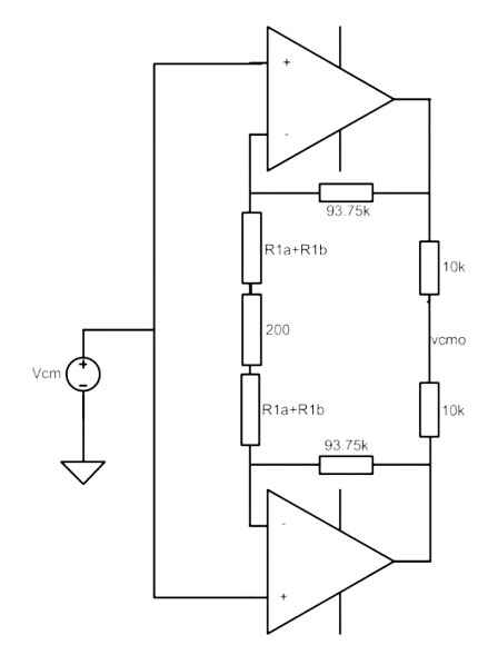
Figure 4 shows the details of the instrumentation amplifier. In this case we have written a ’1’ to Bit 15 of the Config1 register (0x4) which is further illustrated in Figure 1. The200ohms in the center is the input tap for the PEAL system and differential filters. These resistors are also held at a specific voltage corresponding to the fast common mode rejection loop. Resistor R2 is always 93.75k. Resistor R1 is broken up intoR1a+R1b+100 ohms such that the total R1 is set according to the table below excluding the 100 ohms.
We can set the resistor values in the differential input amplifier stage using the following table:
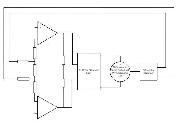
Figure 5 shows the conceptual differential gain which includes a differential integrator in the feedback path of the differential amplifier.
We will begin with use of the AIS339 without use of the 3rdorder programmable filter. To make use of this configuration do not connect the filter capacitors between C1A and C1B orC2A and C2B. Leave these pins floating, do not GROUND or device will not function!
The differential frequency response transfer function is given in the case without the Bessel filter by:
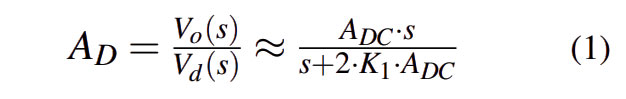
Where K1 is given by:
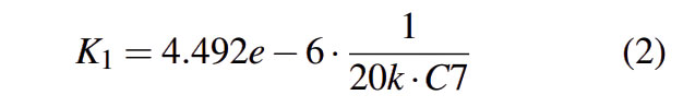
where C7 is the capacitor connected from C7A to C7B.
The low end high pass filter cutoff frequency created by the integrator loop will be:
For example if we maximize the gain according to the tables for the 1st and 3rd gain stages (36db-1.94db) and add the filter flat band gain of 17.8db) then our total gain is 36db+18db+17.8db=71.8db, and we make C7 a 680nFcapacitor then we can expect a corner frequency of about0.2Hz. The corner frequency can be lowered by either increasing C7 or reducing the gain.
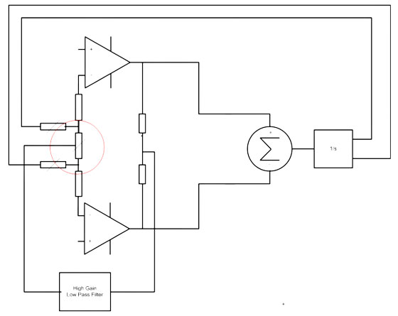
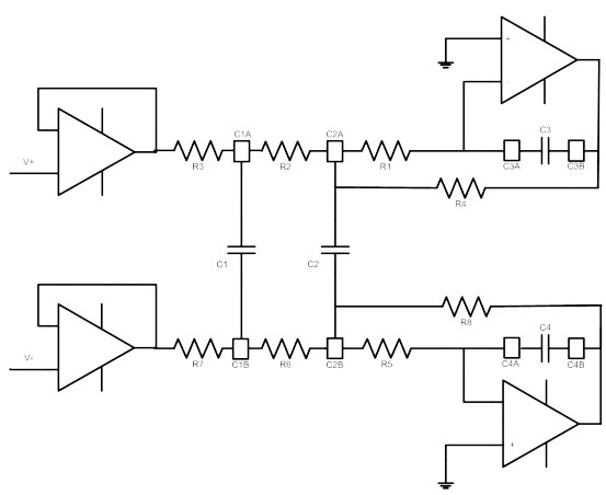
Figure 6 above shows the AIS339 concept without the 3rdorder filter or R2 feedback resistors. The input INA’s can be seen with each of their outputs tied to a common divider. This divider will extract the common mode from the outputs of the amplifier and remove it from the input through a fast PI loop controlling a special voltage supply which sets the common mode between the two segments of the R1 resistor.
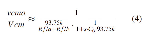
Figure 7 shows the equivalent circuit for the fast CMRR rejection amplifier (labelled High Gain Low Pass Filter in Figure 7). The output divider is buffered and fed into Rfla and the output of the amplifier is used to set the midpoint of the 200Ω resistor with a fixed gain constant. The loop is programmable using the Fast Loop Register Bits C0-C7. BitsC0 to C3 set the Rfa resistor and C4 to C7 set the Refb resistor. Capacitor C6 should be connected between the pins C6A toC6B.
By placing this loop into the feedback it will invert in the transfer function (poles become zeros and vice versa), producing a common mode attenuation for higher gain settings(from the center of the 200ohm input PEAL resistors to the divider at the output of the input instrumentation amplifier stage) of:
For lower gain settings we need to consider the INA gain resistances R1 and R2.
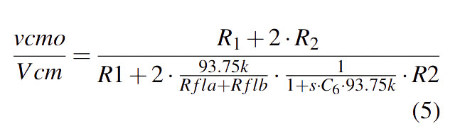
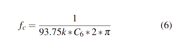
The corner frequency is at:
The combination of Raflb and Rfla can be set according to the following table:
The resulting value for Rfla+Rflb is a combination of the MSB and LSB registers corresponding to Rflb and Rfla. For example a value of 00010001 would result in an overall Rfla+Rflb of 1.5k. A value of 10001000 would result in an overall Rfla+Rflb of 76k+18.7k=94.7k.
It is worth noting that the 200ohm differential resistor used to reject common mode can have its center point moved by a potential related to the voltage supply range as:
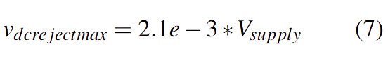
For example, with a 3.3V supply rail we can subtract off a DC input offset of 6.94mV from the common mode.
Differential Operation without Bessel Filter with RLD
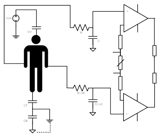
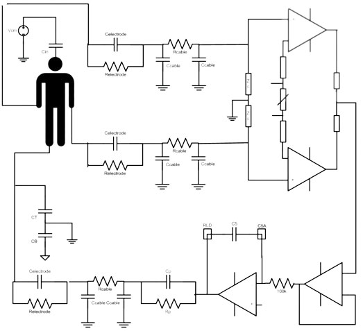
To understand common mode rejection Figure 8 illustrates the basic divider from the common mode voltage source through a capacitance (such as from building wiring and lighting through the air to the subject). This is the potential that appears on the subjects body for example.
Assuming for a moment that local ground and isolated ground are at the same potential we can find a simple formula for that potential, ignoring for the moment ∆C and ∆R:
If the components are completely matched the common mode rejection is high, however, if there are mismatches the common mode turns into a differential mode signal and the common mode rejections degrades.
The common mode rejection can be approximated by:
If the RC bandwidth is about 6Hz and we have 1% matching components then we only have about 73dB of CMR. In reality there are many components that will combine to create a mismatch of 20% or more and therefore degrade our CMR beyond acceptable levels. We need to find a better way.
A more realistic RLD scheme is shown in Figure 9. Here we have modelled the impedances related to the electrode sand cables, as well as finite input impedances of the input amplifiers. Accurate modelling of the mismatches in these components and ensuring the poles are cancelled by zeros in each of the cable and electrode paths is required to use the RLD to optimize the loop CMR.
3rd Order Differential MFB
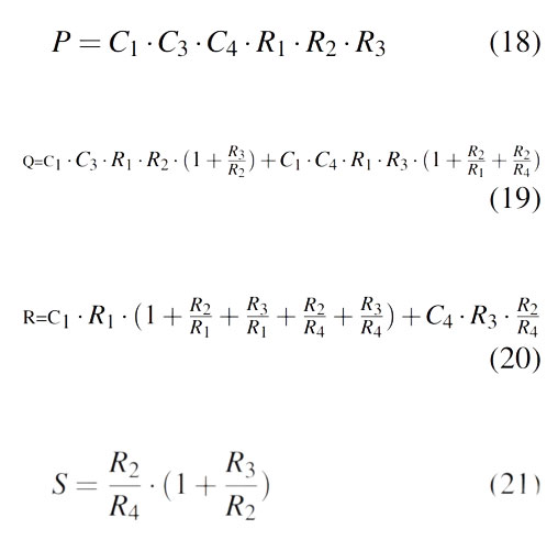
The AIS includes a 3rd order MFB (multi-feedback filter). In this section the equations related to this filter are explored and an example set of component values presented. In the second section a special case of a Bessel filter is derived and component values calculated for an example case which maybe extended to other types of filters in similar way based upon their characteristic polynomial.
The AIS339 includes an MFB filter. This filter can be configured by external capacitors C1, C2, C3 and C4with integrated resistors internally provided and matched. Specifically, R3=750, R2=1.12k, R3=25k.
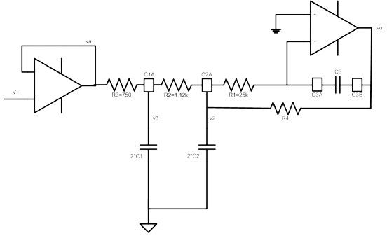
To analyze this circuit we look at the half circuit so that we can analyze it relative to ground. The half circuit requires that we double values of C1 and C2 to reach the same transfer function that we would if we analyzed the entire differential circuit.
By nodal analysis:
Therefore,
Summing the current at node v2:
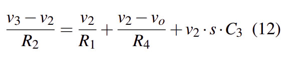
Separating the voltages:
Substituting v2 we obtain:
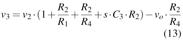
Now summing currents at node v3:
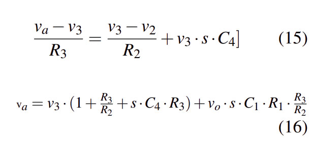
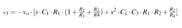
Solving we find the transfer function:
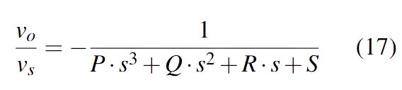
where the coefficients P, Q, R, S are given by:
Dividing through by P, we get:
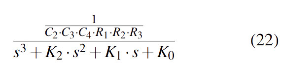
Where,
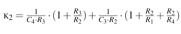
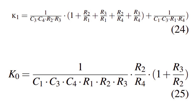
This can be simplified to:
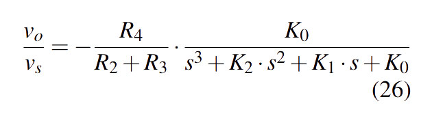
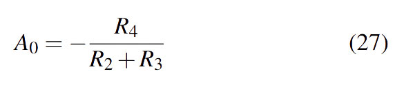
Therefore the DC gain is:
The procedure to follow is:
1. Select a DC gain value, A0 according to R4/R2+R3. With external components such as a resistor across R4 we can reduce but not increase the gain, however, the matching coefficient will be poor due to the difference between on chip and off chip temperature coefficients. 1. Work out the type of filter one wants to use and obtain its characteristic equation coefficients. 2. Use the formulas below for the coefficients to solve the for the components values for an approximately 1Hz bandwidth. 3. Scale the capacitor values to adjust the filter bandwidth to the desired 3dbfrequency or unity gain frequency. 4. Identify the capacitors common to the two halves of the differential circuit and halve the value of these components when used in the differential configuration. 5. Use a numerical solver, such as http://sim.okawa-denshi.jp/en/Multiple3tool.php. Enter the component values and confirm the filter response is as expected. Iterate the corner or unity gain frequency with this tool by scaling the capacitor values.
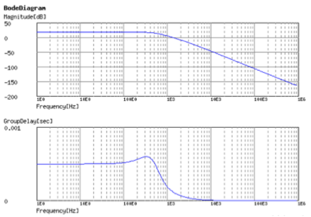
Utilizing the above procedure capacitor values ofC1=15nF,C2=10nF, and C3=C4=2.2nF are obtained. To utilize these values in teh Okawa tool above we need to double the value of C1 and C2 and ensure that we are substituting components into the simulator according to Okawa’s setup diagram and not our own convention. Doing this we obtain the following bode plot:
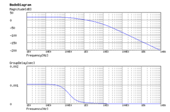
The 3db is at 161Hz and the gain is -7.75 (17.79db). The unity gain frequency is 1176Hz.
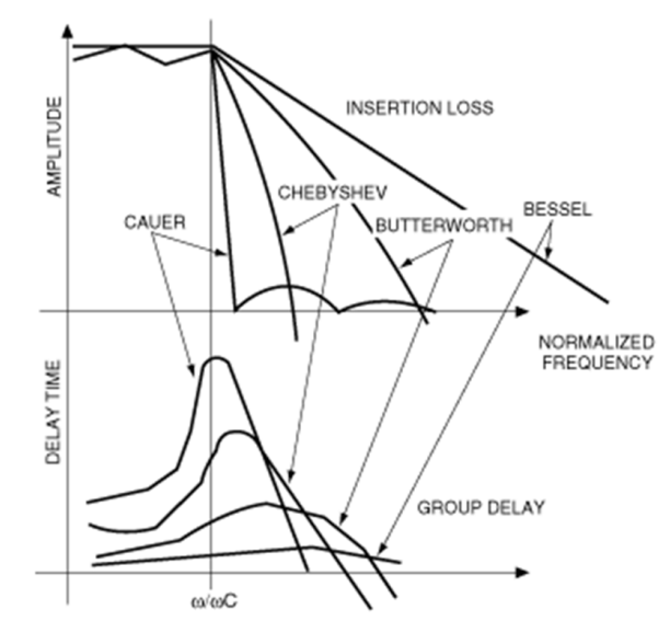
Bessel Filter
Most heart rate waveform extraction systems prefer a Bessel or all pass response. Figure 13 illustrates the difference between a Bessel filter and other types of filters.
In general, it has been shown that a Bessel response will be achieved if the polynomical coefficient are calculated as follows:
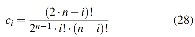
For a 3rd order system of the form c3s2 +c2s2 +c1s+c0 this means that:
c0=15
c1=15
c2=6
c3=1
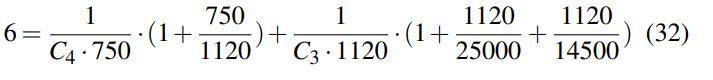
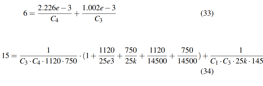
We know that R3=750Ω, R3=1.12kΩ and R3=25kΩ.
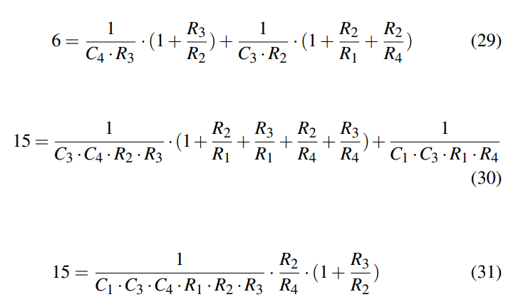
We know that the values of the built in resistors on the IC are R4=14.5k, R3=750, R2=1.12k, R1=25k. This means that the DC gain, A0=R4/R2+R3=14.5k/1870 = 7.75or17.79dB.
Substituting resistor values:
which simplifies to:
which simplifies to:
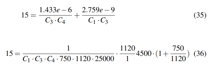
This simplifies to:
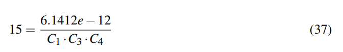
Solving for C1 we get:
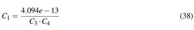
Substituting C1 into 37 we get:
Note that the coefficients we used correspond to a maximally flat response, unfortunately Bessel systems do not have a simple formula to relate pole values to bandwidth.
The poles of a 3rd order Bessel system as given by the coefficients Equation 28 are:
r1 = -2.322 rad/s r2 = -1.8389 - j1.7544 rad/s r3 = -1.8389 + j1.7544rad/s
Bessel poles lie on a family of ellipses becoming larger with increasing order, but all with their near focus at the complex plane origin and the other focus on the positive part of the real axis. We need to divide the roots r1,2,3 by a w3n or 3db frequency to normalize to 1Hz bandwidth. For our application we then need to scale the bandwidth to our desired w3h (our 3db frequency) as desired, ie:
The easiest procedure to do this is to calculate our approximately1Hz bandwidth and then iterate the pole locations by scaling perequation 40.
For example we choose C4=1mF. This results in a C3=0.173mF and C1=2.366µF. Now we multiply by 0.5e-3 to scale the capacitors as follows: C4=0.5µF, C3=0.0685µF and C1=1.183nF.
The wH was set at 2π · 513Hz to create an approximately flat all pass response up to 2π · 250Hz. The easiest way to iterate the wH is to use the tool at http://sim.okawa-denshi.jp/en/Multiple3tool.php. Be sure to be mixed up by the labelling conventions used on this website vs. those used in the analysis as they are not the same.
Now that we have worked out the half circuit capacitor values we need to remember to half the values again for the differential case. Note that only C3 and C4 are connected between the two half circuits and therefore these are the only components whose values have to double.
Finally, we have the following values for the capacitors:
C4=0.25nF (halved)
C3=34nF (halved)
C1=C2=1.183nF (not halved)
The 3db frequency is 513Hz and the gain is -7.75 (17.79db). The unity gain frequency is 1327Hz. We then find that:
Transconductor Mode
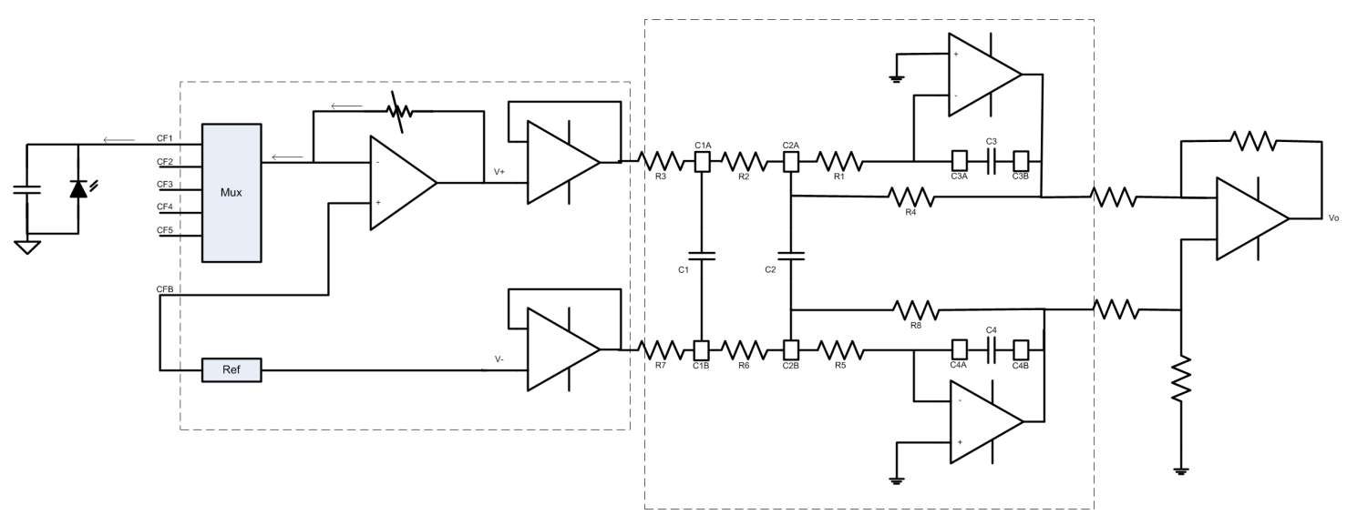
Figure 15 above illustrates the AIS339 reconfigured into Transconductor Mode. In this mode the CFx pins may be connected to up to five different photodiodes while retaining the capture, filter and digitization abilities of the AIS339. The transconductor includes a variable resistor which can be used to control the current gain. The on board precision reference is buffered to VINN which is used as the connection point for the photodiodes and the transconductor inputs. The on board precision reference also represents one of the inputs to the 3rdorder MFB filter. This filter is then coupled to a differential to single ended output stage and finally can be buffered to a nanalog output or can be digitized and read through the SPI registers
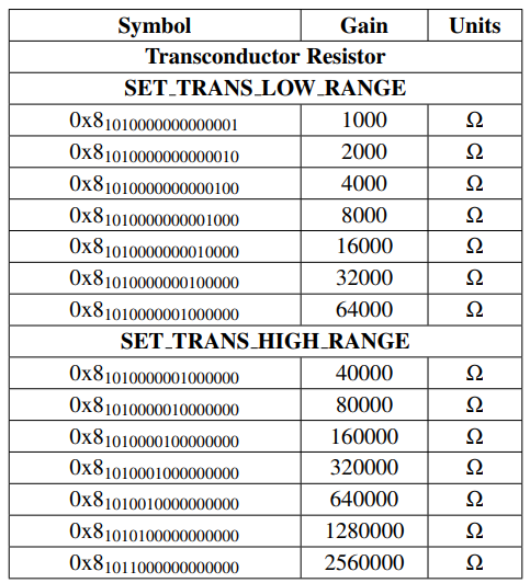
To reduce the number of external components, high valued resistors are included on chip and may be programmed using register 0x8 according to the settings in Table 5.
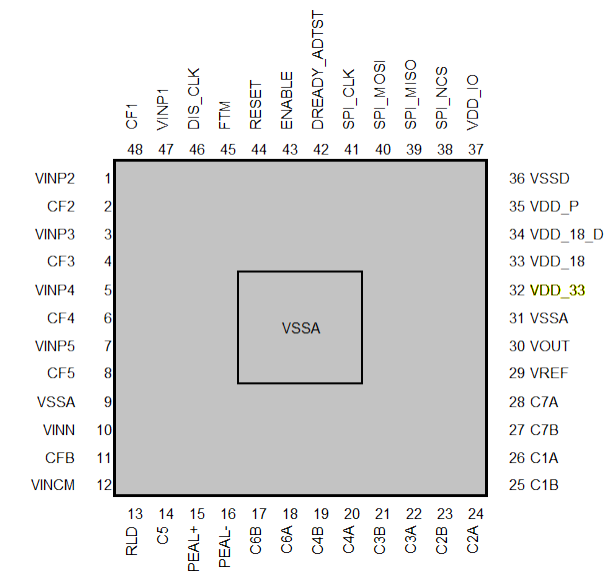
Pinout